The brief
Move from the detail of a real electronic assembly to a semiconductor material concept, explaining organized structure and tunable conductivity.
Audience: educators, technical communicators and subject specialists creating a concise semiconductor materials film.
The visual approach
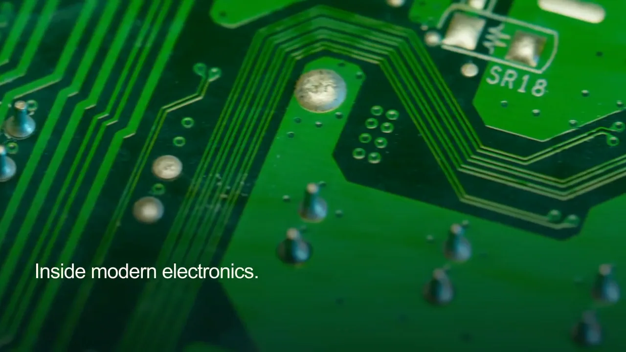
00–06s: A close cropped view reveals the detail of a filmed electronic assembly. 06–12s: The foreground lattice comes closer while distant nodes remain in view. 12–18s: A differently colored node contrasts with the surrounding illustrative lattice. 18–24s: A luminous charge-inspired path crosses the dimensional lattice.
The pulse composition uses a 96 BPM rhythm selected for this storyboard. On-screen words stay short so the semiconductor materials imagery carries the sequence.
Review and editable scope
A real production brief would keep the semiconductor materials subject, source attribution, exact narration and caption wording available for review. A subject specialist must approve the factual explanation before using it in a real lesson.
The studio production plan keeps the four shot selections, crop, title, narration, captions and sound design separate. These notes document how this authored film was made. Use the Martius feature documentation for the product editing and review workflow.
Sources and interpretation
The electronic assembly is illustrative stock, not semiconductor fabrication footage or proof of a specific material. A regular illustrative lattice and arbitrary particles are used. This is not a silicon atomic geometry, transistor design, fabrication recipe or electrical simulation.
The linked NIST: semiconductors resource supports the conceptual topic. Stock subjects are illustrative and are not Martius customers, endorsements or evidence of a named facility’s practices. Original illustration is marked as conceptual wherever its appearance could be confused with observed data.
Scene-by-scene transcript
00–06s — A close cropped view reveals the detail of a filmed electronic assembly. On-screen text: Inside modern electronics.. Narration: Semiconductor materials underpin modern electronics. Original stereo score.
06–12s — The foreground lattice comes closer while distant nodes remain in view. On-screen text: Look inside the structure.. Narration: Silicon is one widely used semiconductor material. Original stereo score.
12–18s — A differently colored node contrasts with the surrounding illustrative lattice. On-screen text: Conductivity can be tuned.. Narration: Its electrical behavior can be tuned. Original stereo score.
18–24s — A luminous charge-inspired path crosses the dimensional lattice. On-screen text: From material to technology.. Narration: These materials enable complex integrated circuits. Original stereo score.
Words, sound and scene notes
- 00:00
- A close cropped view reveals the detail of a filmed electronic assembly. On-screen text: Inside modern electronics.. Narration: Semiconductor materials underpin modern electronics. Original stereo score.
- 00:06
- The foreground lattice comes closer while distant nodes remain in view. On-screen text: Look inside the structure.. Narration: Silicon is one widely used semiconductor material. Original stereo score.
- 00:12
- A differently colored node contrasts with the surrounding illustrative lattice. On-screen text: Conductivity can be tuned.. Narration: Its electrical behavior can be tuned. Original stereo score.
- 00:18
- A luminous charge-inspired path crosses the dimensional lattice. On-screen text: From material to technology.. Narration: These materials enable complex integrated circuits. Original stereo score.